Key Takeaways
- A cold plate is flat. The component side of a power board is not. Component heights on the same board differ on the millimeter scale.
- Whatever gap is left between them fills with air, at about 0.026 W/m·K. Aluminum is roughly 200 W/m·K and copper roughly 400 W/m·K. That air layer is the bottleneck in the thermal path.
- Of the four common thermal interface material (TIM) types, only a pre-formed thermal pad absorbs millimeter-scale height differences while also insulating electrically, die-cutting to shape, and allowing rework.
- Pad thickness is set by the mechanical stack-up, not by the thermal budget. Once thickness is locked, higher thermal conductivity is how you bring thermal resistance back down.
- There is no off-the-shelf thermal pad for a power board. Outline, thickness, and cutouts all follow the board. Good Gi die-cuts thermal pads in house instead of sending them to an outside converter.
Why the Power Shelf Is Moving to Cold Plates
As AI racks move to liquid cooling, most of the engineering attention goes to the GPU side: how the cold plates mount and how coolant gets in and out. But the same rack has another assembly that is getting harder to cool with air: the power shelf.
The power shelf is the group of power supply units that converts incoming power into DC power for the compute trays. As rack power keeps climbing, these shelves are moving from fans to cold plate liquid cooling. Once a cold plate goes on, the engineering question becomes very basic: how does heat from the components on the PCB get into the cold plate?
This article covers that middle layer. Good Gi supplies silicone thermal pads for a liquid-cooled power shelf program at a major power supply manufacturer.
A note on terms: thermal pads are also called thermal gap pads or silicone thermal pads. All of these refer to a pre-formed, compressible TIM supplied at a fixed thickness. They are different from dispensed gap fillers, which are applied as a paste and usually cure in place.
Why Do You Need a Material Between the Components and the Cold Plate?
A cold plate is a metal plate with internal flow channels. Coolant runs through it and carries the heat away. What it has to contact is the component side of the PCB.
The problem is that the component side is not a flat surface.
On a single power board, the MOSFETs, synchronous rectifiers, PFC inductor, transformer, and capacitors all have different package heights. Add component height tolerance, placement tilt, PCB warpage after the board is screwed down, cold plate flatness, and the mechanical tolerance stack, and the cold plate is not pressing onto a plane. It is pressing onto uneven terrain.
Every one of those gaps fills with air.
Air conducts heat at about 0.026 W/m·K. For comparison, aluminum is around 200 W/m·K and copper around 400 W/m·K. Even a thin, invisible layer of air between a component and the cold plate becomes the hardest step in the entire thermal path. No matter how well the device conducts heat or how much coolant flows through the plate, the heat gets stuck at that layer.
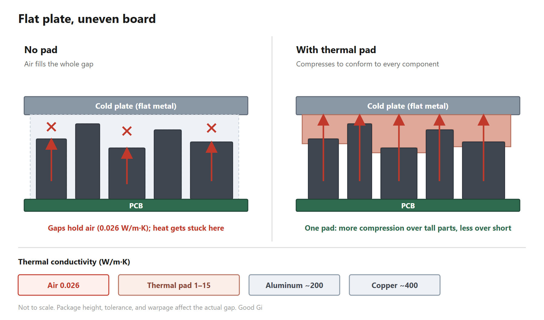
The cold plate is flat; the component side is not. With no interface layer, the whole gap is air (0.026 W/m·K) and heat gets stuck there. With a thermal pad, the same cold plate presses down and the pad compresses more over the tall components and less over the short ones, so every component stays in contact.
That middle layer has to do three things at once:
| Requirement | Why it matters |
|---|---|
| Fill the gap | Component height differences are on the millimeter scale, so the material has to compress and conform to each component. |
| Conduct heat | Once it fills the gap, it has to carry heat. Swapping air for another insulator does not help. |
| Insulate electrically | Component cases often sit at a voltage, while the cold plate is metal and usually grounded. The layer has to withstand that potential difference. |
Together, those three jobs are what a thermal interface material (TIM) does. For where this layer sits in the full cooling loop, see How cold plate modules connect: two piping types between the CDU and the chip.
Thermal Pad vs. Thermal Paste, Gel, or Phase Change Material: Which Fits a Power Shelf?
TIMs come in several forms, and the four common types behave very differently:
| TIM type | Strengths | Limitations |
|---|---|---|
| Thermal grease (TG series) | Can be applied very thin, with the lowest interface resistance | Limited gap-filling ability, so it suits surfaces that already mate closely. Risk of pump-out and dry-out under long-term thermal cycling. Bond line thickness in production depends on dispensing equipment. Messy to clean during rework. |
| Two-part thermal gel (TF series) | Fills irregular shapes and works with automated dispensing in high-volume production | Requires dispensing equipment plus handling and cure time, so the adoption hurdle sits on the production line. |
| Phase change material (PCM) | Softens and wets out above its phase change temperature, combining a thin bond line with low thermal resistance | Has to heat up before it works. Not convenient for disassembly and rework. |
| Silicone thermal pad (TP series) | Pre-formed in selectable thicknesses. Compresses to absorb millimeter-scale height differences. Electrically insulating. Die-cuts to any shape. Reworkable and easy to assemble by hand. | The thicker the pad, the higher its thermal resistance. This is the main trade-off with pads, and it drives the rest of the selection. |
Now look at the power shelf requirements: multiple components on one board, all at different heights, cases at a voltage, assemblies that must come apart for rework, and consistency in volume production.
- Thermal grease cannot fill millimeter-scale height differences.
- Gel and PCM each come with their own process requirements and are less flexible than a pre-formed pad when the board design changes.
- Only a pad covers all of it at once: it compresses, absorbs the height differences, insulates, and can be cut to whatever shape the board needs.
So for this program the answer was a pad. The real decision was which pad. Full part numbers and specifications for all four TIM types are on our Thermal Interface Materials page.
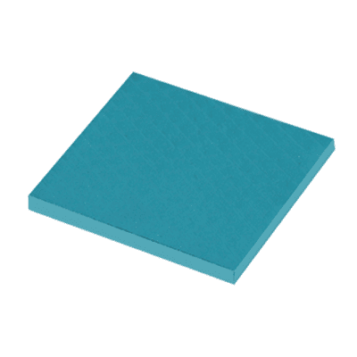
Silicone thermal pads ship as sheet stock. The outline, thickness, and cutouts are set by the board and formed by die-cutting.
How High Should Thermal Conductivity Go? Why This Program Used a 15 W/m·K Pad
A simple way to think about a thermal pad's thermal resistance is in two parts: the bulk resistance of the material itself, plus the contact resistance at the interfaces on both sides. Bulk resistance is roughly thickness divided by thermal conductivity. Thickness is in the numerator, and conductivity is in the denominator.
The catch is that thickness is not ours to choose.
The mechanical design sets pad thickness. How far apart the tallest and shortest components are, how much compression the assembly provides once it is screwed down, and how much margin the worst-case tolerance stack requires: work those out and the thickness follows. Too thin, and the tallest component bottoms out the pad while the shortest never makes contact. Too thick, and the compressive stress goes straight into the components and their solder joints.
So when the mechanical design locks the thickness and it cannot go any thinner, the only variable left is the denominator: thermal conductivity.
For this program, the selection was TP-1500, the high-conductivity grade in our TP series of silicone thermal pads, rated at 15 W/m·K. At the same thickness, its bulk thermal resistance is about one-fifth that of a typical 3 W/m·K pad. The mechanical design set the thickness, so conductivity had to make up the difference.
Is a Higher-Conductivity Thermal Pad Always Better?
No. High-conductivity pads get there by loading the silicone with large amounts of thermally conductive filler, and that has direct costs:
- More filler makes the pad harder and less compressible. Reaching the same compression takes more clamping force, and that stress ends up on the components and solder joints.
- Density goes up, and so do weight and cost.
- A pad that is too hard cannot conform to the height differences, which puts you back where you started, with gaps that are not filled.
Softer with lower conductivity, or firmer with higher conductivity: that trade-off has to be worked out again on every board. No single part number fits every design.
Why Datasheet Values Are Not Enough: Test on the Actual Board
All of the reasoning above ends in the same place: the numbers only count once the pad has actually been compressed on the board.
The same pad can perform very differently on different boards. At a minimum, the result depends on:
- Actual component height distribution and tolerances
- Clamping force and screw torque, which set the compression
- Cold plate flatness and stiffness
- Compression set over long-term use
- Assembly method on the line and the number of rework cycles
The thermal conductivity on a datasheet is a material property measured under standard test conditions. It is not the thermal resistance on your board. What matters is how many degrees the temperature drops with this pad, at this thickness and this size, on this board, torqued to this spec.
Thermal pads are also almost never off-the-shelf parts. Outline, thickness, cutout locations, and which components to clear are different on every program. They are custom parts by nature.
In practice, the selection process looks like this: define the outline, cut samples, test on the board, change the thickness or material, cut new samples, and test again.
How fast the program moves depends less on the datasheet than on how long one loop takes.
How Long Does One Sample Loop Take?
NVIDIA CEO Jensen Huang has described a standard he calls the "speed of light." The speed of light is a physical limit that nothing can exceed, so instead of asking how to beat yesterday's time, he asks what the physical limit of a process is. Speaking to NVIDIA employees in Taiwan in May 2026, he contrasted shaving a day off a 63-day process with finding out that the same process could take 7 days. The first is barely worth the effort. The second is worth getting excited about (Economic Daily News, in Chinese).
This is not a requirement aimed at any one supplier. It is the pace of the industry, and it runs all the way down the AI server supply chain. At the far end, it turns into a very concrete question: when will the pad the engineer needs be on their bench?
Thermal pads start out as large rolls or sheets. Turning them into a shape that matches the board and clears specific components takes die-cutting.
When die-cutting is outsourced, every loop picks up waiting time: the cutting die has to wait its turn to be made, the cut parts have to ship back, and every dimension change starts the cycle over. What should be a simple cutting job becomes several days per loop once scheduling and shipping are added. Worse, it pushes engineers to test only one option at a time, because every extra variant means another wait.
How In-House Die-Cutting Changes Thermal Pad Sampling
Good Gi has in-house die-cutting equipment for thermal pads. Send us dimensions or a drawing, and we cut and ship samples directly, with no outside converter in the loop.
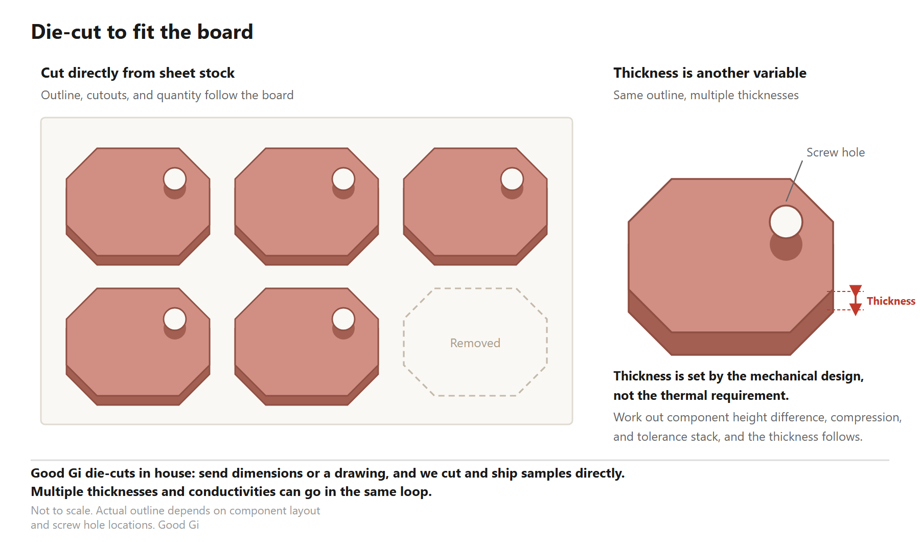
The value is not just a few days saved. It changes how you select a pad:
| Outsourced die-cutting | In-house die-cutting | |
|---|---|---|
| Time per loop | Tooling, queueing, and round-trip shipping add days to every loop | Scheduled as soon as dimensions arrive and run on in-house production time |
| Variants per loop | Usually one, because every change means another loop | Multiple thicknesses and conductivities can go in the same loop |
| Basis for selection | Estimate from datasheets, verify, and start over if the estimate is wrong | Select directly from measured results on the actual board |
Sample turnaround was one of the reasons this customer brought Good Gi in for the prototyping stage. Material specs can be compared on paper. Whether samples reach the engineer on the program's schedule cannot. That comes down to whether the cutting equipment is in the supplier's own plant.
Back to the speed of light: moving a sample loop from waiting on an outside converter to in-house production time is the part that pushes 63 days toward 7.
Frequently Asked Questions
When should I use thermal paste instead of a thermal pad?
It depends on the gap. If the two surfaces already mate closely and the gap is under 0.1 mm (0.004 in), thermal paste (grease) can be applied thinner and gives lower interface resistance. Once you need to bridge millimeter-scale component height differences, paste cannot fill the gap and you need a compressible pad. Rework is the other deciding factor: for modules that have to come apart for service, pads are much cleaner than paste.
Is a pad with higher thermal conductivity always better?
No. High conductivity comes from heavy filler loading, which makes the pad harder and less compressible and raises density and cost. A pad that is too hard cannot conform to component height differences, and the resulting gaps can increase thermal resistance instead of lowering it. Evaluate conductivity together with thickness, hardness, and compression. Higher conductivity is the lever to use when the mechanical design has locked the thickness and it cannot go any thinner.
How do I choose thermal pad thickness?
The mechanical design sets it, not the thermal requirement. Work out the component height distribution and tolerances, the compression available after the assembly is screwed down, and the worst-case tolerance stack, and the thickness follows. In practice, engineers usually test two or three thicknesses side by side and choose based on measured temperatures and how the assembly goes together. That is why sample turnaround directly affects the program schedule.
Can thermal pads be custom cut to my board's dimensions, thickness, and cutouts?
Yes. For power boards, they are custom parts by nature. The outline follows the component layout, the cutouts follow the screw holes, and the thickness follows the component height differences and available compression. Pads ship as sheet stock and are die-cut to shape. Good Gi die-cuts thermal pads in house, so we can cut directly from your dimensions or drawing.
Are thermal pads, thermal gap pads, and silicone thermal pads the same thing?
Yes. They are different names for the same category: a pre-formed, compressible thermal interface material supplied at a fixed thickness. They are different from thermal grease, which is spread on, and thermal gel or gap filler, which is dispensed onto the part.
What information do you need to quote thermal pad samples?
Four things: the component height difference (between the tallest and shortest components), the compression space available after assembly, the clamping force or screw torque, and the target temperature. With those, we can prepare samples in matching thicknesses and conductivities. If your design is still in progress, we can start by talking through pad selection.
Can I get samples before placing an order?
Yes. Because thermal pads are custom parts, we recommend sampling at the actual dimensions and testing on the board from the start instead of comparing datasheets alone. Tell us the component height difference, available compression, and target temperature, and we will arrange samples.