Nanocrystalline Selection: PSU & Wireless Charging EMI Success
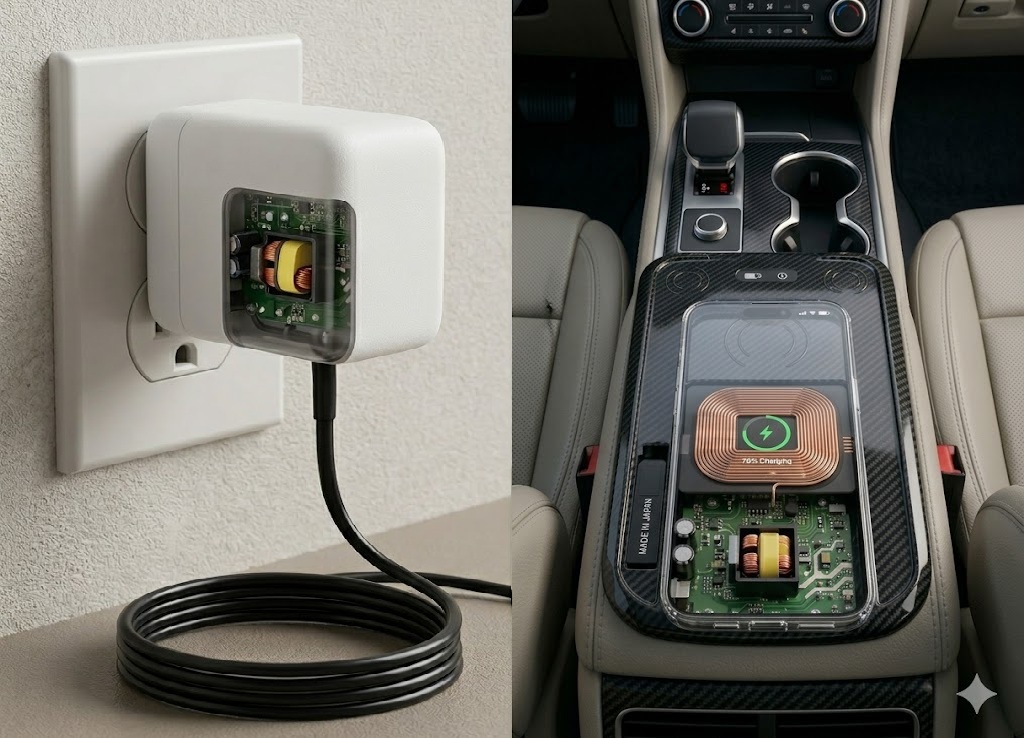
Application Background: EMI Interference Challenges in High-Density Power Structures
During the development of wall-mount adapters and automotive wireless charging pads, the combined electric and magnetic field interference between magnetic components (e.g., transformers) and AC pins is a critical EMI issue that R&D engineers must prioritize.
As product designs evolve toward miniaturization, high power density, and high integration, internal space becomes increasingly cramped, significantly raising the difficulty of EMI control.
When the distance between the transformer and AC pins is too short, magnetic and electric field interference tends to leak through the pins, causing conducted emissions (150kHz–30MHz) and radiated emissions (30MHz–300MHz) to exceed regulatory limits.
Using traditional shielding materials without considering insulation and dielectric strength can lead to reliability risks, such as short circuits at the pins or ESD (Electrostatic Discharge) breakdown.
Therefore, achieving a balance between dielectric strength, safety, and high-efficiency shielding within limited space is key to passing safety standards and EMI testing.
In this case, the client evaluated the integration of our Multi-layer Nanocrystalline Composite Tape into wall-mount models to achieve a feasible EMI improvement solution without significant structural changes or excessive costs.
Customer Field Test Feedback: EMI Improvement Verification via Nanocrystalline Composite Tape
To verify the shielding effectiveness of the material in actual models, the client conducted conducted and radiated EMI tests on wall-mount power supplies, comparing data performance and shielding efficiency before and after integration.
| Test Items | Conditions / Description |
|---|---|
| Test Model | Wall-mount Power Adapter |
| Test Environment | EMI evaluation for Conducted Emissions (150kHz–30MHz) and Radiated Emissions (30MHz–300MHz) |
| Evaluation Metrics | Comparison between EMI regulatory limits and interference shielding effectiveness |
| Original Issue | Crosstalk between the transformer and AC pins, causing EMI levels to exceed limits. |
| Solution | Two samples of Nanocrystalline Composite Tape:: Sample 1:Reflective shielding layer at the bottom (closer to the source). Sample 2:Reflective shielding layer at the top. |
| Test Results | After implementing GQ-NAB10000 sample 1 showed superior shielding effectiveness and significant EMI improvement. |
The focus of this test is to compare the differences in EMI conduction and radiation suppression effects when the reflective shielding layer is placed in different positions. The results show that the overall shielding effectiveness is more significant when the reflective shielding layer is positioned at the bottom, closer to the interference source (Sample 1).
Sample 1: Bottom Reflective Shielding Layer
Sample 1 utilizes a stacking configuration of a bottom reflective shielding layer + top multi-layer nanocrystalline + black insulation film. This structure positions the shielding layer closer to the primary interference source, facilitating earlier noise blocking and path redirection.
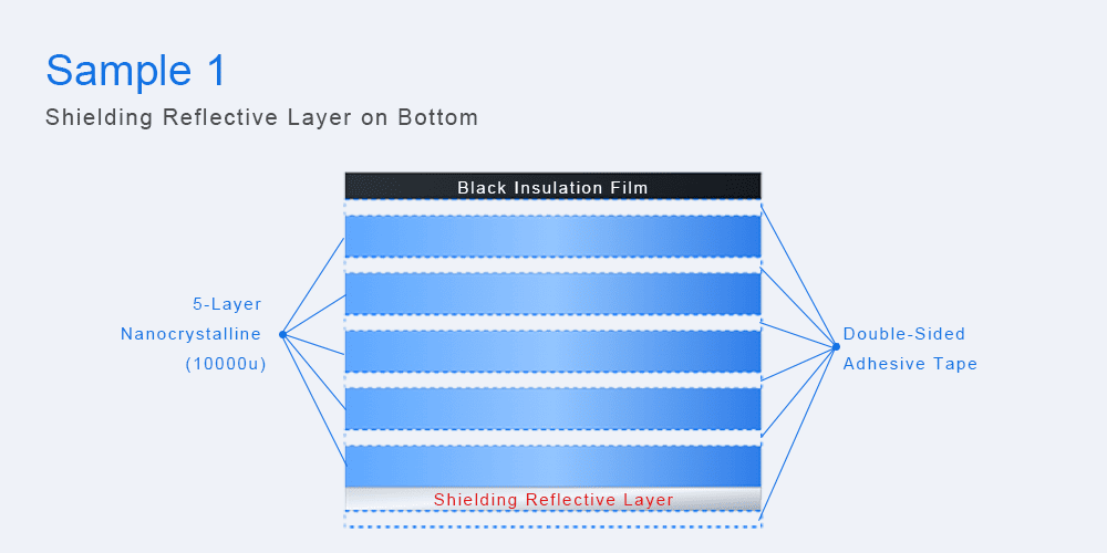
Figure: Sample 1 Schematic, Reflective Shielding Layer on Bottom.
Sample 2: Reflective Shielding Layer at the Top
In Sample 2, the reflective shielding layer is positioned at the top. This contrasts with Sample 1 to evaluate the impact of different layer arrangements on EMI shielding effectiveness.
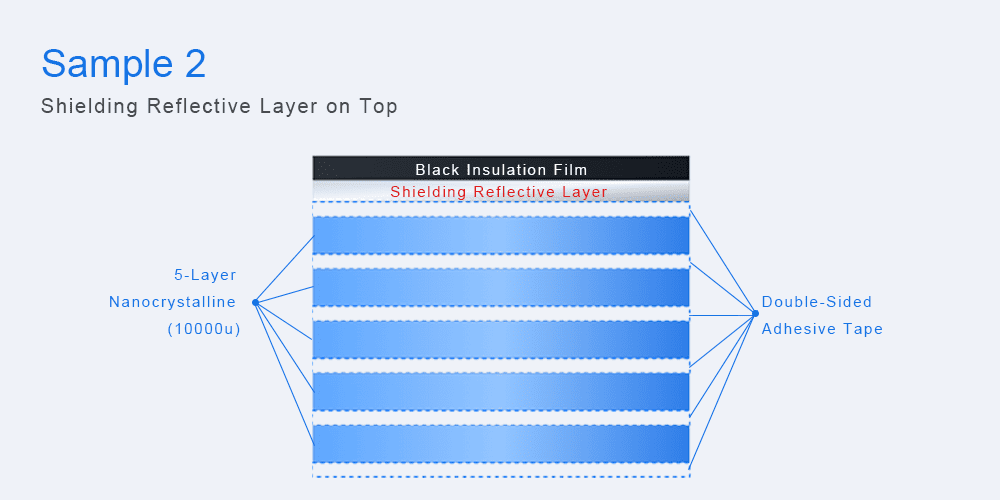
Figure: Sample 1 Schematic, Reflective Shielding Layer at the Top
Bonding Method Schematic
Besides the material stacking structure, the bonding position and coverage area also directly affect EMI improvement. The figure below illustrates the bonding method of the nanocrystalline tape in the transformer and AC Pin areas.
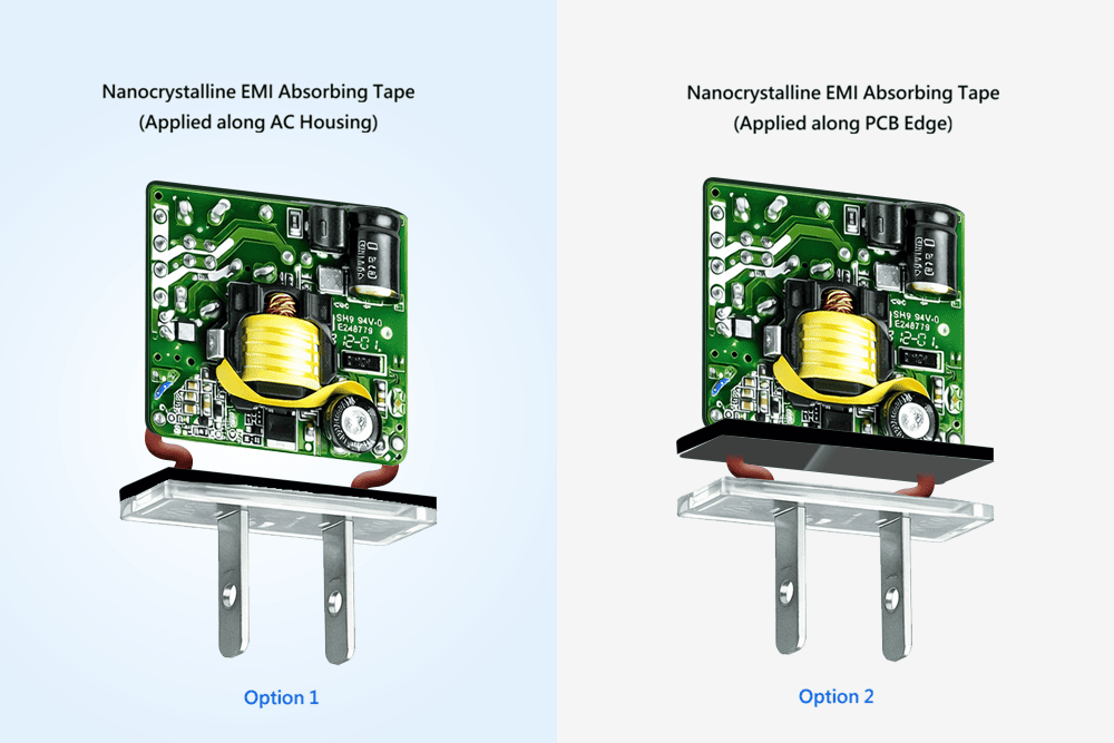
Figure: Bonding Method of Nanocrystalline Tape in Transformer and AC Pin Areas
After confirming the effective shielding capability of the 5-layer 10,000u structure, based on the successful results of Sample 1, the client is further evaluating reducing the 5 layers to 1 or 3 layers. They are also testing variable samples with different magnetic permeabilities (such as 5000u) to identify the optimal solution balancing performance and cost.
Key Engineering Observations: Impact of Magnetic Permeability, Bonding Position, and Structural Design
From these test results, it is observed that the EMI improvement of nanocrystalline tape depends not only on the material itself but also heavily on its bonding position, coverage area, and return path design. Key engineering observations are as follows:
- Higher permeability enhances high-frequency shielding: Upgrading from 5000u to 10,000u nanocrystalline material improved electromagnetic shielding in the target high-frequency bands, effectively suppressing complex EMI noise.
- Composite structures facilitate interference return paths: When the shielding layer and mechanical parts form an overlapping design, it creates a superior return path for combined electric and magnetic interference, effectively addressing conduction and radiation issues.
- Bonding area and position directly impact shielding effectiveness: Compared to applying tape only at the AC pins, bonding at the transformer side and increasing the coverage area more effectively blocks crosstalk coupling paths.
Engineering Value for Clients and Reasons to Choose This Product
The value of this product lies not only in reducing EMI data but also in its thin, processable, and mass-producible form, helping engineering teams achieve safer and more cost-effective design improvements within existing structural constraints.。
Enhancing Reliability and Safety
The nanocrystalline composite tape features an integrated insulation layer, preventing short-circuit risks from metal shielding contacting mechanical parts while reducing the likelihood of ESD (Electrostatic Discharge) breakdown
Solving Complex Interference and Overcoming Space Constraints
For products with limited internal space, this tape provides a passive, thin, and easy-to-apply EMI solution, significantly reducing design modification costs and integration barriers.
| Material Characteristics | Engineering Benefits |
|---|---|
| Ultra-high Magnetic Permeability (10,000) | Provides stronger magnetic field shielding, effectively suppressing high-frequency noise and improving EMI test performance. |
| Wide Operating Temperature Range (-40°C ~ 110°C) | Suitable for power supplies with high heat dissipation requirements and more demanding automotive wireless charging environments. |
| Flexible Tape Form and Multi-layer Structure | Allows customized adjustment of nanocrystalline layers based on component location and interference levels, achieving the optimal balance between performance and cost. |
Conclusion: A Mass-Producible Shielding Solution Balancing EMI Performance, Safety, and Cost
This case study confirms that integrating Nanocrystalline Composite Tape into high-interference areas of wall-mount units effectively mitigates conducted and radiated emissions across the 150kHz–300MHz frequency range. By combining an insulating design with a multi-layer nanocrystalline structure, the engineering team successfully balanced EMI shielding, safety, and manufacturing feasibility within limited space.
- Effectively shields conducted and radiated interference within the 150kHz–300MHz frequency band.
- Reduces the risk of short circuits and ESD breakdown through insulation and multi-layer structural design.
- Assists RD engineers in finding EMI improvement solutions that balance both performance and cost control.
- Suitable for high-frequency interference equipment such as power supplies, wireless charging pads, and power electronic systems.
For product development projects that need to balance EMI improvement, structural constraints, and mass production integration, this material serves as a highly efficient electromagnetic shielding solution with practical engineering flexibility.